
English 
T: +86-13760465505
E: vibetop@163.com
E: vibetop@163.com
No.13, Cheng Guang Industrial park, Dafu Community, GuanLan Street, Longhua District, Shenzhen, GuangDong, China

Views: 0 Author: Site Editor Publish Time: 2026-06-30 Origin: Site


Advanced semiconductor packaging pushes operational boundaries daily. Wide-bandgap devices like Silicon Carbide and Gallium Nitride face rapidly escalating thermal densities. They demand superior heat management to survive under extreme power loads. Standard cooling solutions now hit severe physical limits. Base metals like aluminum simply cannot move heat fast enough to prevent thermal runaway. This harsh reality forces engineers to pivot toward high-purity copper components for advanced cooling. These advanced materials dictate the ultimate performance ceiling of your entire fabrication process. Selecting the correct alloy ensures stable electrical conductivity and prevents catastrophic equipment failures.
We need a rigorous evaluation framework to navigate this critical shift. You must learn to specify and source semiconductor-grade copper without falling for exaggerated supplier claims. This guide delivers precise criteria for evaluating material purity, manufacturing methods, and strict compliance standards.
Material Purity Dictates Performance: Oxygen-Free High Thermal Conductivity (OFHC) copper and specific alloys (e.g., C14500) are non-negotiable for preventing vacuum outgassing and maintaining electrical consistency.
Manufacturing Method Impacts Yield: The choice between CNC machining, additive manufacturing, and sintering directly affects thermal resistance and structural integrity.
Compliance is a Baseline, Not a Feature: True semiconductor readiness requires strict adherence to SEMI standards, verifiable metallurgical reporting, and controlled surface finishing.
Copper serves as the default material for solving next-generation thermal and conductive problems. You cannot rely on traditional materials for modern chip architectures. Modern fabrication plants demand absolute precision. Base metals fail under these extreme parameters. High-purity copper guarantees the necessary thermal runway for advanced processing.
Wide-bandgap (WBG) semiconductors create severe thermal bottlenecks. Silicon Carbide (SiC) and Gallium Nitride (GaN) operate at much higher frequencies and voltages than traditional silicon. They generate intense localized heat during normal operation. You must dissipate this heat rapidly. Superior heat dissipation ensures these components maintain their projected operational lifespans. Without rapid cooling, WBG devices suffer premature failure. They literally burn themselves out from the inside.
Engineers must navigate strict electrical versus thermal trade-offs continuously. We often look at the International Annealed Copper Standard (IACS) to measure electrical conductivity. High IACS values usually correlate with excellent thermal conductivity. However, foundries often add alloying elements to improve machinability. These specific additions degrade thermal performance significantly. You must balance the need for easy machining against the demand for maximum heat transfer.
We also must view alternative materials through a skeptical lens. Novel synthetic materials exist today. Diamond composites and advanced graphite solutions show promising laboratory results. Yet, bulk copper remains the most scalable solution available. It offers highly verifiable performance metrics. Foundries rely on it for massive volume production. Synthetic alternatives struggle to match copper's proven reliability in real-world fabrication scenarios.
You must categorize cooling solutions based on specific copper grades. Fabrication equipment and advanced packaging require distinct metallurgical profiles. We cannot use a one-size-fits-all approach. Let us examine the dominant alloys utilized across modern facilities.
Oxygen-Free High Thermal Conductivity (OFHC) copper represents the industry gold standard. We deploy it primarily in deep vacuum environments. It builds exceptional deposition equipment and high-end thermal straps. The total absence of oxygen prevents hydrogen embrittlement. This dangerous condition occurs when hydrogen reacts with oxygen in standard copper at elevated temperatures. It causes catastrophic structural failure. OFHC guarantees the highest thermal and electrical baseline available anywhere.
Tellurium copper provides an excellent engineering compromise. We use it to machine intricate semiconductor copper fittings. It also creates high-speed CNC machined connectors and contact pins. Tellurium copper retains roughly 85% of pure copper’s electrical conductivity. Crucially, it offers drastically improved machinability. Pure copper acts sticky and frequently gums up cutting tools. The tellurium addition creates shorter chips during cutting. This unique property allows for complex geometries and faster production cycles without compromising quality.
Sintered copper paste transforms modern die attach processes. We use it to bond semiconductor dies directly to their substrates. Copper sintering creates superior thermal pathways compared to traditional solders. However, we must implement a reality check here. Sintering introduces complex thermo-mechanical stress across the assembly. The process requires highly stringent control protocols. You must manage temperature profiles perfectly. Mistakes during sintering cause micro-voiding and eventual die delamination.
Material Grade | Primary Advantage | Thermal Conductivity Limit | Typical Application |
|---|---|---|---|
OFHC Pure Copper | Zero oxygen outgassing | Maximum capability | Vacuum chambers, deposition |
C14500 Tellurium Copper | Superior machinability | ~85% of pure copper | Complex connector pins |
Standard Aluminum | Lightweight, easy cutting | Insufficient for WBG | Low-power heat sinks |
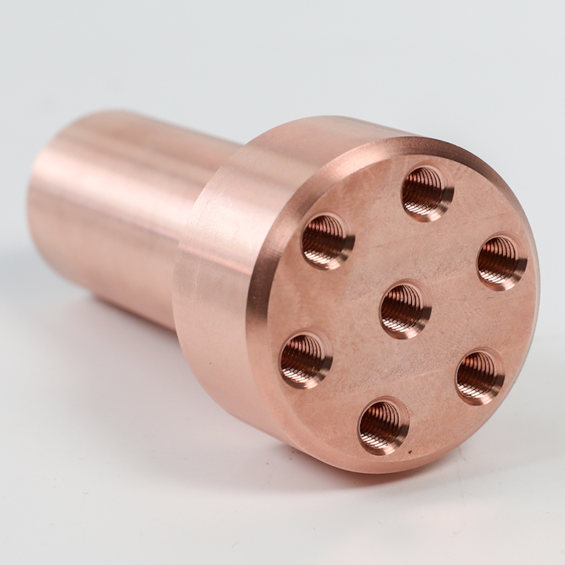
How a manufacturer makes a part dictates its final performance in the field. We must evaluate these dimensions carefully. Every manufacturing method carries inherent risks. You must match the production technique to the specific thermal requirement.
CNC machining remains the backbone of component fabrication. It delivers an unmatched surface finish. We need absolute flatness for mating surfaces in thermal transfer applications. Any microscopic gap traps air and ruins thermal conductivity. The primary risk involves severe tool wear. Machining pure copper causes galling. The soft metal smears directly onto the cutting tool. You need specialized cooling fluids and tailored feed rates. Poor machining practices lead to severe surface contamination and rejected parts.
Additive manufacturing unlocks radical new thermal designs. Engineers now 3D print pure copper components successfully. This method enables complex conformal cooling channels. Subtractive machining simply cannot hollow out these curved internal pathways. However, printing carries distinct limitations. The as-printed surface roughness usually fails semiconductor vacuum standards. You almost always require secondary CNC operations to smooth these surfaces. Furthermore, internal porosity remains a verifiable risk. Microscopic voids disrupt thermal pathways and trap process gases.
Thermal straps provide essential flexibility for delicate machinery. We use them for critical vibration isolation. Cryogenic coolers generate continuous mechanical vibrations. These vibrations easily destroy sensitive semiconductor optical arrays. Copper thermal straps bridge the gap effectively. They transfer heat efficiently while absorbing mechanical shocks. We assemble them using hundreds of fine OFHC copper foils. This layered construction ensures maximum flexibility without sacrificing thermal conductivity.
Sourcing specialized components demands a strict shortlisting logic. You cannot treat these items as standard hardware. We need a verifiable vetting process. Selecting the wrong vendor jeopardizes the entire fabrication line.
You must demand full material lot traceability from every vendor. Do not accept generic compliance statements. Material test reports (MTRs) must prove the exact elemental composition. They should not merely list broad alloy families. If a supplier cannot trace their copper back to the original mill, disqualify them immediately. Impurities measured in tiny parts per million can ruin an expensive vacuum chamber.
Cleanliness dictates operational success in fab environments. We require strict protocols before parts ever leave the factory.
Cleanroom Packaging: Vendors must use Class 100 or Class 1000 cleanrooms for final inspection.
Ultrasonic Cleaning: Components must undergo rigorous ultrasonic baths. This removes microscopic machining oils and metallic debris.
Oxidation Prevention: Suppliers should ship parts in specialized inert bagging. Exposure to ambient air degrades surface purity rapidly.
Precision requires verifiable proof. You must highlight the necessity of Coordinate Measuring Machine (CMM) reports. We inspect these specific reports for absolute flatness and parallelism. Thermal interfaces do not tolerate micro-gaps. Even a tiny deviation reduces the contact area dramatically. This forces heat to travel through trapped air. Accurate dimensional metrology eliminates these invisible thermal barriers.
Defect Type | Root Cause | System Impact |
|---|---|---|
Surface Oxidation | Improper inert bagging | Increased thermal resistance at interfaces |
Micro-Porosity | Poor 3D printing parameters | Trapped gases released into vacuum |
Galling Marks | Incorrect CNC feed rates | Loss of mating surface flatness |
Buyers need a clear map for implementation. Sourcing Copper Semiconductor Spare Parts carries unique technical challenges. We must identify red flags early during the procurement cycle.
Beware of suppliers making broad, unsubstantiated performance claims. Warn your team against vendors who cannot provide precise thermal conductivity variances. Copper behaves differently across distinct operating temperatures. A reliable supplier knows exactly how their specific alloy performs at 200°C versus 20°C. Vague data sheets indicate a severe lack of semiconductor-specific expertise.
Never rush directly into high-volume manufacturing. We strongly recommend starting with low-volume CNC runs. You must validate the thermal performance in real-world conditions. Build a proof-of-concept assembly first. Test it thoroughly before committing to hard tooling. This phased approach prevents massive losses when scaling up intricate semiconductor copper fittings.
Global commodity markets fluctuate wildly. You must assess your supplier's raw material resilience. Can they source pure OFHC copper consistently? Ask about their strategic inventory buffers. A robust partner maintains strong relationships with premium copper mills. Weak supply chains lead to sudden material substitutions. You cannot afford unauthorized alloy changes in delicate semiconductor applications.
Specifying high-performance components requires careful balancing. We must weigh thermal demands against practical machinability. Vacuum-compatibility realities also dictate our final material choices. Engineers cannot rely on outdated assumptions when managing next-generation heat densities.
Here are the critical next steps for your engineering teams:
Audit your current thermal bottlenecks to identify exactly where standard aluminum heat sinks fail.
Request comprehensive material certifications and CMM reports from all potential new suppliers.
Initiate a dedicated proof-of-concept run for your most critical cooling components.
Establish clear communication regarding surface finish and cleanroom packaging requirements before signing any contracts.
A: Standard copper contains trace amounts of oxygen. In high-temperature vacuum chambers, this oxygen reacts with hydrogen gases. The reaction creates steam bubbles inside the metal. This phenomenon, called hydrogen embrittlement, fractures the component. It also causes severe vacuum outgassing. OFHC copper contains virtually zero oxygen. It eliminates these catastrophic risks entirely while delivering maximum thermal conductivity.
A: Yes, you can use aluminum for lower power density areas. It weighs less and machines easily. However, aluminum has a significantly lower specific heat capacity and thermal conductivity than pure copper. Advanced wide-bandgap devices generate massive, highly localized heat. Aluminum cannot pull this heat away fast enough. Copper becomes strictly essential for these extreme environments.
A: The physical machining process leaves bulk thermal conductivity unchanged. However, poor machining creates a rough surface finish. High Ra values prevent flush mating between components. They introduce tiny air gaps at the thermal interface. Air acts as a powerful insulator. This trapped air drastically increases overall thermal resistance across the assembly.
A: Tellurium copper sacrifices approximately 10% to 15% of its IACS electrical conductivity compared to pure OFHC copper. In exchange, it provides a massive increase in machinability. Pure copper tears and galls during cutting. Tellurium copper allows for clean, precise threading and high-speed production yields. It serves as an ideal compromise for complex connector geometries.


